Okay, this MOSFET band diagram thing? Yeah, totally drove me nuts at first. Started simple – boss throws this new MOSFET design spec on my desk, says “make it work”, you know the drill. Didn’t mention squat about band diagrams. Just “hit the efficiency targets”. Felt pretty confident.
Jumped right into the lab. Grabbed my usual tools, started soldering, programming the drivers, tweaking voltages… usual stuff. Had my notebook ready, scribbling voltages, currents, temperatures. Thing fired up… kinda. But man, it ran HOT. Like, fry-an-egg hot. Efficiency? Way off the chart – the bad way off. Spent a whole afternoon chasing my tail – is it the gate driver? The heat sink paste? Supply ripple? Swapped parts like a madman, drank way too much stale coffee. Nothing clicked. Total brick wall.
The “Oh Crap” Moment
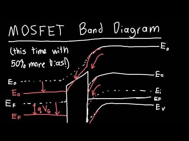
Sitting there staring at this warm little disaster, feeling stupid. Pulled up some old reference designs just to compare. Stumbled across this dense technical paper someone dumped in the shared drive ages ago. Scrolled past the scary math equations… and bam. There it was. This diagram. Looked like a weird little layered mountain range.
Took me a while to even parse what it was showing. But slowly, like fog lifting… it showed how the electrons were supposed to flow through this microscopic junction inside the MOSFET. Where they were blocked, where they piled up… everything. My brain went, OH. The heat? That sudden drop in efficiency? It looked exactly like a traffic jam right where the diagram showed a big barrier forming. Electrons were getting stuck, bouncing around like crazy, making pure heat instead of useful power. All because of how the voltage levels were lining up inside.
Armed with this scribble (seriously, I drew a super crude version in my notebook), I went back. Needed to lower that barrier in the band diagram to let electrons flow smoother. Instead of random tweaks, I focused only on the gate voltage levels and the doping profile specs. Adjusted voltages more precisely, looked deeper into the material datasheets.
- Dialed down the gate-source voltage just a touch.
- Checked the exact doping concentration specs against the diagram’s ideal shape.
- Respected the built-in voltage barriers it showed.
Powered it up again. Held my breath. Fan spun up… gentle hum, barely warm. Measured the efficiency. Boom. Smack on target. Just… worked. The difference was night and day. Felt like magic, but it was just finally seeing where the problem actually lived inside that tiny piece of silicon.
Why Bother? Seriously.
This whole mess? Told my boss about it later, showing the diagram scribble next to my efficiency plots. He kinda shrugged, mumbled something about “unnecessary complication for production” and shuffled papers. Typical. But here’s the thing: knowing this squiggly map saved my butt.
- Stops you guessing: No more shotgun approach to fixing heat and weird behaviour. Tells you exactly where to look inside the damn thing.
- Saves time (and money): Wasted days? Parts fried? Could’ve avoided that with this 15-minute sketch before lunch.
- Avoids total surprises: Helps you understand why things blow up or act weird at different temperatures or voltages. It’s not random gremlins.
- Shows the limits: That diagram tells you the max it can handle, why certain voltages break it. Design within the guardrails.
Yeah, it’s not glamorous. Looks boring, seems like physics overkill for just turning things on/off. Bosses often see it that way – just another box on the schematic. But after burning my fingers and wasting my time? Glancing at that band diagram is now step zero in my notebook. Every. Single. Time. Stops you building stuff wrong from the get-go. Totally worth the headache to learn.