Alright, so I wanted to share a bit about my journey with MOSFETs, specifically digging into their structure. It wasn’t like I woke up one day and decided, “Hey, I need to become a semiconductor physicist!” Nah, it was way more about things just not working right, and me getting fed up.
I was tinkering with a project, trying to control some power, you know, the usual DIY stuff. And these MOSFETs, they were supposed to be simple switches, right? That’s what everyone says. But mine were either getting super hot for no reason I could see, or they weren’t switching as cleanly as I expected. Sometimes they’d just give up the ghost entirely. Poof.
My first big mistake was probably thinking they were just like those beefy mechanical relays, but faster. I’d look at the schematic symbol, three legs, seemed straightforward enough. But then I’d glance at a datasheet and my eyes would glaze over. So many parameters!
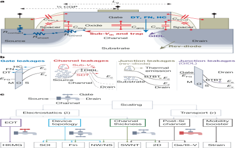
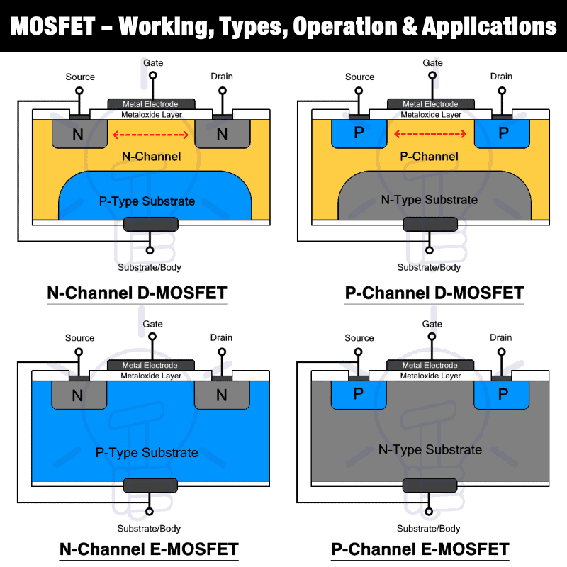
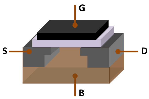
So, I started from the very basics. I literally typed “mosfet structure how it works” into a search engine. What I found was a bunch of diagrams with layers. You got your Source, your Drain, and the all-important Gate. But then there was this other thing, the Body or Substrate. That already threw me for a loop. Why is it there? What does it do?
Digging into the Layers
I spent a good chunk of time just staring at those cross-section diagrams. Trying to visualize it. Here’s what I sort of pieced together, in my own clumsy way:
- You have this silicon base, the substrate.
- Then you have these two regions, the source and drain, made of a different type of doped silicon.
- Between them, under the gate, is the channel region. This was the magic part for me.
- The gate itself is isolated from the channel by a super-thin layer of oxide. Like, incredibly thin. It’s amazing that this even works without current just punching through.
My process was pretty messy. I didn’t have a fancy lab. I was mostly looking at stuff online, reading application notes (the ones that weren’t too academic, anyway), and trying to connect it back to the problems I was having. For example, I learned that when you apply a voltage to the gate, it creates an electric field. This field is what forms or enhances the channel, allowing current to flow between the source and drain. No current actually flows into the gate in an ideal DC situation, just charges it up like a tiny capacitor. This “capacitor” idea helped me understand why gate drivers are a thing, especially for switching fast.
Then there’s the body diode. Oh man, this one got me good a few times. I always thought a MOSFET, when off, blocked current in both directions, and when on, conducted. But nope, there’s this intrinsic diode between the drain and source (well, technically body to drain, but often body is tied to source). It’s just there, part of the structure. If you’re driving an inductive load, like a motor, this diode can be a lifesaver (for freewheeling current) or a pain if you’re not expecting it or if it’s not robust enough.
I remember trying to pick a MOSFET for a slightly higher power application. I was looking at Rds(on) – the resistance when it’s on. I noticed that different MOSFETs, even with similar voltage and current ratings, had vastly different Rds(on) values. Looking at the structure helped me understand, at least vaguely, that it’s related to how wide and short that channel can get, and the density of charge carriers. Bigger silicon die usually means lower Rds(on), but also higher capacitance, which means it’s harder to switch fast. It’s all a trade-off, isn’t it? Just like everything in engineering.
It wasn’t a quick “aha!” moment. It was more like a slow dawning. I’d read something, it wouldn’t make sense. Then I’d try to build a circuit, blow something up (again), go back, read some more, and then a little piece would click into place. Like, understanding that the gate voltage doesn’t just turn it on or off like a switch, but actually controls the conductivity of the channel. More voltage (up to a point) means a better channel, lower resistance.
So yeah, getting a handle on the basic MOSFET structure wasn’t just some academic exercise for me. It actually helped me make better choices in my projects, understand why things were failing, and generally be less clueless. It’s still a super complex field, and I’ve only scratched the surface, but even that little bit of understanding made a big difference. It’s like knowing a little bit about what’s under the hood of your car – you might not be able to rebuild the engine, but you can at least understand why it’s making that funny noise.