Alright, let’s talk about something I’ve been digging into lately: MOSFETs and FinFETs. You hear these terms thrown around, especially when new chips and gadgets come out, and for a while, I was just nodding along, you know? But then I decided, no, I actually want to understand what the fuss is all about, at least from a practical point of view. This isn’t going to be some super deep dive into semiconductor physics, just what I’ve picked up trying to make sense of it all.
Starting with the Old Faithful: MOSFETs
So, my journey started with the good old MOSFET. Metal-Oxide-Semiconductor Field-Effect Transistor. Sounds like a mouthful, right? But the way I got my head around it was thinking of it like a tiny, tiny switch or a faucet. You’ve got a path for electricity to flow, and then you’ve got this “gate.” Apply a little voltage to the gate, and boom, the switch turns on, current flows. Remove the voltage, it turns off. Pretty straightforward. For decades, this was the king. Everything from your ancient calculator to slightly less ancient computers ran on these things. They were reliable, relatively easy to make (in the grand scheme of things), and they did the job.
I remember looking at basic circuit diagrams, and these little symbols were everywhere. They were the building blocks. And for a long time, the game was just to make them smaller. Smaller MOSFETs meant you could cram more onto a chip, make things faster, and hopefully use less power. Simple, right? Well, not quite.
The Shrinking Problem
Here’s where things started to get a bit hairy, from what I gathered. As these MOSFETs got shrunk down to really, really tiny sizes – we’re talking nanometers here – they started to act up. The main issue I kept reading about was “leakage.” Imagine your faucet. Even when you turn it off, if it’s old and worn, it still drips. These super-small MOSFETs were doing the same with electricity. They couldn’t turn off completely. The gate just didn’t have enough control over that tiny channel where the current flows. This meant wasted power, more heat, and just general inefficiency. Not good when you’re trying to make a phone battery last all day or stop your laptop from frying an egg.
I tried to picture it: the gate is trying to pinch off the flow, but because everything is so small and the electric fields are all over the place, it’s like trying to stop a firehose with just your thumb. Some water is gonna get through. This was a big roadblock. How do you keep making things smaller and better if the basic switch stops working properly?
Enter the FinFET: A New Dimension
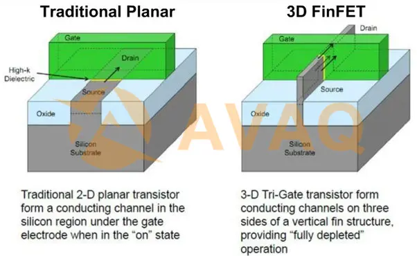
This is where I first properly encountered the term “FinFET.” It took me a bit to visualize. With a traditional MOSFET (often called a “planar” MOSFET), the channel the current flows through is, well, flat, like a road, and the gate sits on top, like a toll booth.
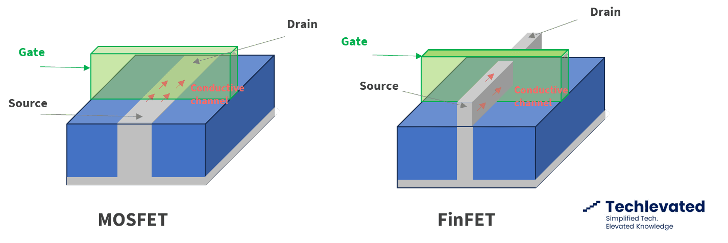
With a FinFET, they got clever. Imagine that road, but now it’s raised up, sticking out like a fin. A shark’s fin, hence the name. And here’s the crucial part: the gate doesn’t just sit on top anymore. It wraps around this fin on three sides!
Suddenly, my mental picture clicked. Instead of the gate just pressing down from above, it’s now got a much better grip on the channel from multiple sides. It’s like going from trying to squeeze a tube of toothpaste with one finger to using your whole hand. Much more control!
- Better Off-State: Because the gate has more control, it can shut off the current flow much more effectively. Less leakage. That dripping faucet problem? Significantly reduced.
- Faster Switching: With better control, you can also switch it on and off faster.
- Lower Voltage: Often, you can get them to work at lower voltages, which again means less power consumption.
My “Practical” Observations
Now, I’m not sitting in a lab with an electron microscope comparing these things side-by-side. My “practice” here is more about observing the real-world impact. I started paying more attention to tech announcements. When a new processor comes out and they brag about “X-nanometer FinFET technology,” I now have a better idea of what they’re talking about. It means they’re using these 3D-gate structures to keep pushing performance and efficiency.
I think about my newer devices. My phone lasts longer than my old ones. My laptop can handle heavy tasks without turning into a furnace. Part of that improvement, I’m pretty sure, comes down to the advancements these FinFETs enable. They’re not the only factor, of course, but they’re a big piece of the puzzle for keeping Moore’s Law sort of, kind of, alive, even if it’s on life support.
The downside? Well, making these fin structures is way more complicated than the old flat MOSFETs. I can only imagine the manufacturing challenges. It’s probably a lot more expensive too, especially initially. But the benefits in terms of performance per watt, especially for high-performance and mobile applications, seem to outweigh the costs for many new designs.
So, MOSFET vs FinFET?
It’s not like MOSFETs are dead. For a lot of simpler, less demanding applications, or where cost is the absolute king and you don’t need the tiniest possible size, traditional planar MOSFETs are still perfectly fine and widely used. They are the workhorses for many things.
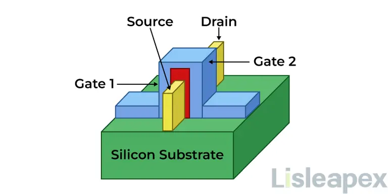
But when you’re talking about the cutting edge – the processors in your flagship smartphone, your high-end CPU or GPU – that’s where FinFETs (and now even more advanced stuff like Gate-All-Around FETs, or GAAFETs, which is a whole other rabbit hole) are taking over. They’re the solution to that “leaky tiny switch” problem.
So, that’s my journey so far in trying to get a handle on these two. From a simple switch to a 3D marvel. It’s pretty cool to see how engineers keep finding ways to push the boundaries. Makes you appreciate the tech in your pocket a little more, doesn’t it?