Alright, so today I’m gonna walk you through my experience wrestling with the small signal MOSFET model. When I first saw it in books, honestly, it just looked like a bunch of complicated math. But, you know, when you’re actually trying to build something like an amplifier and get it to work without it just humming or doing nothing, you kinda have to get your head around it. It wasn’t exactly love at first sight, let me tell you.

First Steps: The DC Bias Point is King
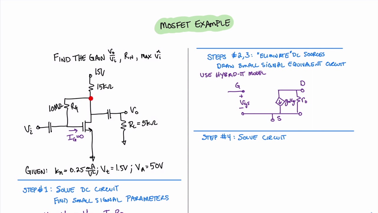
The very first thing I learned, the hard way mostly, was to nail down the DC operating point. You gotta figure out where your MOSFET is sitting electrically when there’s absolutely no AC signal coming in. Is it even turned on? Is it in saturation like it’s supposed to be for an amplifier, or stuck in the triode region? I remember this one time, I spent ages scratching my head over why my amplifier’s gain was pathetic. Turns out, my biasing was all wrong. The MOSFET was barely alive. So, rule number one for me became: get your DC voltages (like VGS, VDS) and current (ID) sorted out first. If that’s off, your small signal model is just a fantasy.
Adding the “Wiggles” – The AC Signal Part
Okay, so once the MOSFET is biased correctly and just sitting there, stable, then we can think about what happens when a tiny AC signal comes along, say at the gate. This is where “small signal” is key. We’re assuming these AC wiggles are small enough that the MOSFET’s behavior around that DC point is pretty much linear. No big swings that push it into weird states.
This is where I started to get a feel for ‘gm’, or transconductance. I’d literally look at the ID versus VGS curve in the datasheet, find my DC operating point (that specific ID and VGS), and then imagine the slope of the curve right at that point. That slope, that’s pretty much your ‘gm’. It tells you how much the drain current (ID) changes if you wiggle the gate-source voltage (VGS) a little bit. A steeper slope means a bigger change in current for the same voltage wiggle, so, a higher ‘gm’. This was a big “aha!” moment for me.
Don’t Forget the Output: Output Resistance ‘ro’
Then there’s the other side of the coin, the output characteristics. Ideally, for an amplifier in saturation, the drain current shouldn’t really change much even if the drain-source voltage (VDS) changes. But real-world MOSFETs aren’t perfect. There’s this effect, channel length modulation, which basically means ID does change a tiny bit with VDS. This gives us the output resistance, ‘ro’. I used to think of ‘ro’ as a measure of how good the MOSFET is at acting like a constant current source. A really high ‘ro’ is generally what you want for voltage gain, meaning the output current is pretty stable despite changes in output voltage. Trying to measure this directly on a breadboard was a real pain, though, lots of things can throw it off.
Building the Simple Model in My Head (and on Paper)
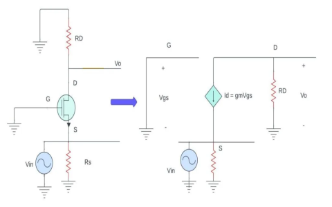
So, with ‘gm’ and ‘ro’ figured out, I could start to piece together a simplified model for AC signals:

- The input (gate to source) for low frequencies pretty much looks like an open circuit. Easy enough. (At higher frequencies, you gotta add capacitors, but let’s not go there for now).
- The output (drain to source) has a current source. The value of this current source is ‘gm’ multiplied by that small AC gate-source voltage (vgs).
- And then, that output resistance ‘ro’ sits in parallel with this current source.
Drawing this out as a little equivalent circuit made things so much clearer. Suddenly, I could analyze amplifier stages without getting bogged down in the full, hairy MOSFET equations. It was like having a simplified map.
Testing it Out: Did it Match Reality?
Theory is one thing, but does it actually work? I remember building a basic common-source amplifier. I calculated the expected voltage gain using the ‘gm’ and ‘ro’ I’d estimated (either from datasheet curves or some quick DC simulations). Then, I grabbed my breadboard, a handful of resistors, a capacitor or two, and the MOSFET. Hooked up my function generator to put in a small sine wave, and watched the output on my oscilloscope.
And you know what? Most of the time, it was surprisingly close! Not spot on, of course. Breadboards have their own gremlins, component tolerances play a part, and my calculations were always a bit rough. But it was definitely in the ballpark. It showed me that this small signal model wasn’t just some academic exercise; it actually helped predict how the circuit would behave. That was a good feeling, made me trust the process a bit more.
So, Why Bother With All This?
You might ask, why go through all this trouble when you can just throw the whole circuit into a SPICE simulator? And yeah, I use SPICE all the time, it’s a fantastic tool. But for me, understanding the small signal model is about getting an intuitive feel for why the circuit behaves the way it does. It helps you design. If your simulated gain is too low, the model gives you clues: Is ‘gm’ too small? Is ‘ro’ killing your gain? Is your biasing off? It helps you troubleshoot and think.
I recall this one project, a custom preamp that sounded absolutely terrible. The previous guy had just kind of thrown components at it. I had to go back to basics, figure out the biasing for each stage, estimate the small-signal parameters, and then I saw it – one MOSFET was barely biased on, its ‘gm’ was practically zero. Swapped out a resistor to fix the bias, and boom, the thing came alive. That’s when it really clicked for me. This stuff isn’t just for passing exams; it’s for making things actually work in the real world.